
Conventional electronics technologies are fast approaching their physical limits at a time when the demand for higher-quality images, faster communications and more compact electronics continues to build.
Light, rather than electrons, is expected to be the information carrier of the next generation of devices, promising higher speeds, power savings and enhanced sensitivity and selectivity. The use of light in such applications is a field of research known as photonics, and A*STAR researchers are making some impressive technological breakthroughs in this area.
The rise of light-emitting diodes
The development of advanced light-emitting diodes (LEDs) is one of the key areas of research at A*STAR. LEDs are rapidly gaining popularity as a next-generation light source. Unlike incandescent bulbs and fluorescent lamps, which generate unwanted heat and non-visible emissions such as ultraviolet light, LEDs produce little heat and emit light in a narrow wavelength band, making them much more energy-efficient. Light in LEDs is generated through a process involving recombination of electrically excited electrons and electron vacancies (holes) in a suitable semiconductor.
LEDs are already available in many consumer and industry applications, ranging from traffic lights to the backlights in flat panel displays. Yet there remain many technological issues that could be improved on, most notably light-emission efficiency and manufacturing cost.
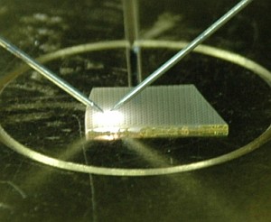
Photograph of a white LED based on the inclusion of quantum dots.
Whiter light with quantum dots
The combination of red, green and blue is familiar to most of us as the three colors making up the pixels in our television sets and computer monitors. Together these three colors can produce any color, including white. LEDs of these three colors can fulfill the same role, but pure white emission in a single package is what is needed for applications such as display backlights. White LEDs are typically fabricated by adding yellow phosphor to a blue LED, which generates a ‘whitish’ light. The color is not perfect because energy losses in the phosphor introduce ‘gaps’ in the color spectrum.
Under the direction of Soo Jin Chua, a professor at the A*STAR Institute of Materials Research and Engineering (IMRE), researchers including Chew Beng Soh and Liu Wei are developing white LEDs that do not include phosphors. They have hit upon the idea of using nanometer-scale semiconductor crystals called ‘quantum dots’ instead.
In their first demonstration of the technology, the team used quantum dots of gallium nitride — the semiconductor on which blue LEDs are based — impregnated with indium atoms. The addition of indium shifts the emission of the quantum dots to yellow wavelengths. A major advantage of this approach is that the quantum dots simply convert a fraction of the photons produced by the LED into another wavelength. “Using our approach, light comes directly from electron–hole recombination, so there is no energy loss in the process,” says Wei.
Already the team has achieved an inherent energy-conversion efficiency of 50%, elevating their technology to the leading ranks in LED research. The overall ‘package’ efficiency, a key gauge of brightness, is about 10%. The figure is lower than that for phosphor-based white LEDs, but “we are working hard to achieve better light extraction,” says Soh.

Blue emission from a prototype organic LED.
Organic blue
White LEDs would not be possible without the invention of blue LEDs, which remain relatively expensive to produce. Zhikuan Chen, senior scientist in the Synthesis and Integration group of the IMRE, has been looking into the use of organic materials as a means of lowering the manufacturing cost of blue emitters.
LEDs are usually made of an inorganic semiconductor compound, such as silicon or gallium nitride in the case of blue LEDs. As Chen notes, however, making LEDs from these crystalline materials is expensive. “Silicon, for example, requires the use of very expensive manufacturing equipment, like that needed for vacuum-deposition at high temperature. Organic materials, on the other hand, can be easily dissolved in solvent, so you can manufacture products using a solution process at low cost,” he says.
Already, researchers worldwide have succeeded in developing organic LEDs (OLEDs) that can emit light at red and green wavelengths. But they continue to struggle to produce stable, highly efficient blue emitters because of a lack of organic compounds with the right electronic energy structure. Chen says that it is difficult to inject sufficient and balanced numbers of holes and electrons into the light-emitting layer of blue OLEDs.
Chen is treading a particularly thorny path to solve this problem. While many of his competitors are working on small molecules, Chen has bet on large molecules, namely fluorene-based polymers and oligomers, for success. Chen explains that large molecules are harder to design, but they are stable and soluble, and so are capable of high emission efficiency. He also avoids small molecules because of the expense involved in manufacturing, which would be equivalent to that needed for silicon.
The approach has started to pay off. Having optimized the materials and device physics, his team recently fabricated a blue OLED with a world record 10.4% package efficiency, well above the 4–6% commonly reported for such devices.
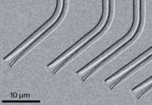
Scanning electron microscopy image of a silicon-based waveguide for coupling optical signals with electronic circuits.
Image courtesy of J.F. Song
Silicon photonics
For Patrick Lo Guo-Qiang, director of the Nano Electronics and Photonics Program at the A*STAR Institute of Microelectronics, silicon matters greatly. Lo and his team are developing tiny silicon-based devices with the aim of constructing a pair of ‘optoelectronic’ transceivers that convert electrical signals into optical ones, and vice versa. He notes that while optical fiber is gradually replacing copper cables in communication networks around the world, “what is important for efficient communication is the connectors between optical fiber and copper fixtures at each end,” he says.
Under the direction of Dim-Lee Kwong, the institute’s executive director, the team’s research in silicon photonics is ultimately aimed at integrating optical and electronic circuits on a single silicon-based chip. Silicon is emerging as an alternative to conventional compounds for optical interconnects, such as gallium arsenic and indium phosphide, because of its abundance and ready integration into existing semiconductor-fabricating technologies. Despite being famous for its poor optoelectrical properties, researchers continue to search for ways to achieve with silicon the same level of performance offered by other compounds.
The team has been developing suites of device building blocks that can be integrated to form transmitters, receivers and other key optoelectronic integrated circuits. Companies must at present purchase different components from different developers to construct devices — an expensive process. A*STAR’s approach is to offer a complete set of building blocks. “Our job is to provide a standardized technology platform. Guided by design rules, product developers can focus on pushing products into useful formats, such as circuit designs,” Lo says. Their recent achievements include the integration of a silicon modulator and a germanium photodetector on silicon, as well as silicon-based waveguides for channeling light through circuits.
“We view silicon photonics today in a very similar light to the integrated electronics industry 40 years ago. Our research is moving in this direction,” Lo says.
About the Institute of Materials Research and Engineering
The Institute of Materials Research and Engineering (IMRE) was established in 1997 with the aim of becoming a leading research institute for materials science and engineering. The IMRE has developed strong capabilities in materials analysis, characterization, materials growth, patterning, fabrication, synthesis and integration, and has established reseach and development program in collaboration with industry partners.
About the Institute of Microelectronics
The Institute of Microelectronics (IME) was established in 1991 with the mission to add value to Singapore’s semiconductor industry by developing strategic competencies, innovative technologies and intellectual property; enabling enterprises to be technologically competitive; and cultivating a technology talent pool to inject new knowledge into the industry.


